The Death of LCDs, Means New Life for Chips
[Opinion] Major moves in recent weeks show that LCD's days are numbered. But it's great timing for semiconductor makers.
Good Evening from Taipei,
Around 20 years ago I was in a media briefing with a senior executive of AU Optronics, then Taiwan’s largest flat-panel maker. LCD displays were hot and the days of bulky cathode-ray tube TVs were numbered.
In that meeting an astute journalist (not me!) asked the AUO boss a snarky albeit fair question: What happens when everyone’s already bought themselves a flat-screen TV, won’t the market tank?
Don’t worry, the executive replied, LCD resolution will continue to advance and these TVs will only last about eight to ten years anyway. Consumers will keep buying.
He was wrong.
It’s only a matter of time before LCD disappears, and three developments this past month have convinced me the end is nigh:
Innolux sold a 5.5G LCD fab in Southern Taiwan to TSMC.
AUO is set to sell two facilities, in Taichung and Tainan, to Micron.
Apple dumped LCD for all future iPhones, according to a Nikkei report this week.
LCDs are more than a century old, but it wasn’t until RCA started tinkering with the technology in the 1960s that it become viable. Product development reached take-off velocity in the 1990s, and by the early 2000s the Three Musketeers of global hardware production — Japan, South Korea and Taiwan — were in a race.
Thanks to an all-industry effort spanning motherglass makers, chemicals suppliers and equipment providers, panel sizes continued to rise. In 2009, Sharp opened a 10G fab in Sakai, near Osaka, with glass substrates measuring 2.9 meters x 3.1 meters, meaning you could easily make huuuge TVs — or a lot of large ones very cheaply. Resolution also advanced, from a paltry 720 to the current 8K, which was first released in 2012.
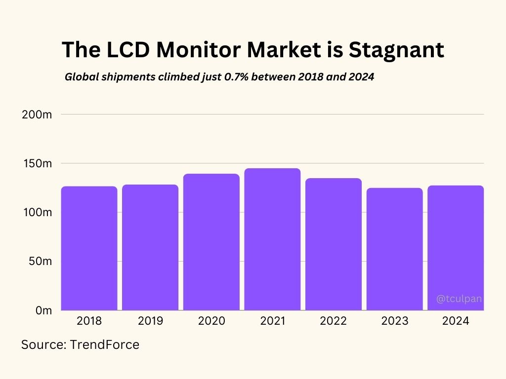
But progress stopped a decade back and that prediction of 20 years ago has fallen flat. Resolution hasn’t budged, it just got cheaper, and LCDs last a long time so consumers aren’t constantly upgrading.
Those who could develop new technologies, like Organic Light-Emitting Diodes (OLED), changed direction quickly and survived — Samsung is the prime example. Those who couldn’t, died: Taipei-based Chunghwa Picture Tubes was one of many. Now, even Sharp is in ill health and that much-celebrated 10G fab in Sakai is set to be mothballed next year. (And to think, Donald Trump once called Foxconn’s proposed 10.5G fab in Wisconsin The Eighth Wonder of the World. Thankfully for Wisconsin taxpayers it never even got built.)
Those stuck in the middle, like Taiwan’s AUO and compatriot Innolux were left with a stagnant market for large-sized panels used in TVs and PC displays, and shrinking demand for smaller sizes like phones. Prices and profits could only fall.
Today, OLED, and its cousin AMOLED, account for the majority of all smartphone screens. LCDs still dominate larger displays, with OLED accounting for just 3.1% of all TVs in 2023. But small form factors always lead the display industry, and larger sizes follow later. Apple started using OLED in its Apple Watch, and now it’s becoming more ubiquitous among the company’s products.
Glass Panels Become Chips
TSMC and Micron buying factories from Innolux and AUO doesn’t mean the chipmakers are getting into the display business. Instead, both are doubling down on high-bandwidth memory (HBM) and preparing for a new wave of chip-packaging technologies. They’re betting on a (glass) panel future.
At SEMICON Taiwan this week, packaging is the hot topic. Executives from TSMC and SK Hynix talked about future trends, and the message is simple: chip packaging is no longer about just adding a ceramic coating and attaching wires. Instead, they need to find ways to take an 8-layer stack of DRAM (ie HBM) and bond it to increasingly complicated processors. TSMC’s approach called CoWoS (Chip-on-Wafer-on-Substrate) is the leading solution. This is helped in large part by the fact that TSMC has a lock on the fabrication of AI chips because it’s the leader in process technology. Intel has something called Foveros and Samsung’s offering is named I-Cube.
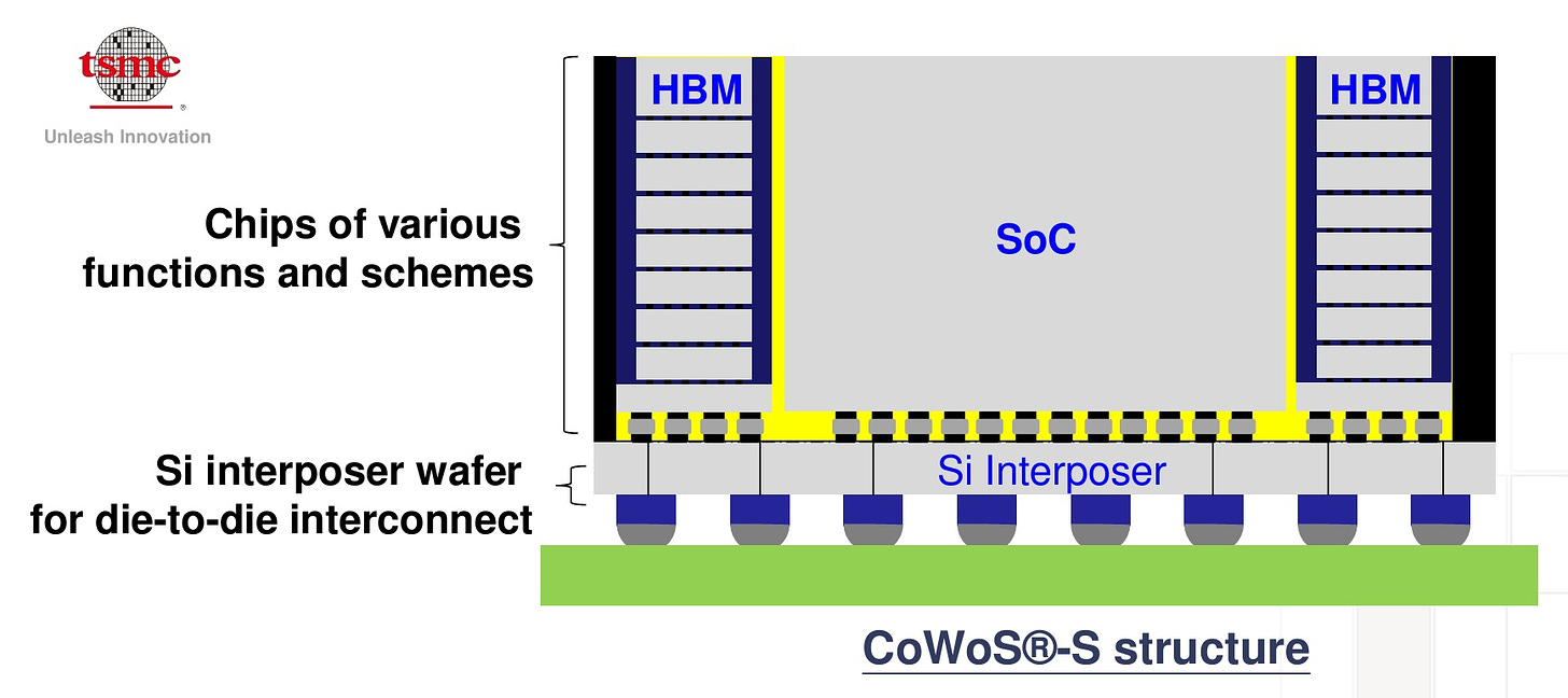
Each of these approaches are remarkably similar, and generally involve sticking individual chips to a silicon interposer through which they connect to their neighbors. This then gets bonded to a substrate which is the part that attaches to a system’s motherboard. TSMC is in such a hurry to expand its packaging capacity that it’s likely to just gut that newly acquired Innolux fab and repurpose it for CoWoS. But it still needs to make a decision about future packaging technologies.
This graphic is taken from a presentation given by TSMC’s VP of R&D Douglas Yu at the HotChips conference in 2021.
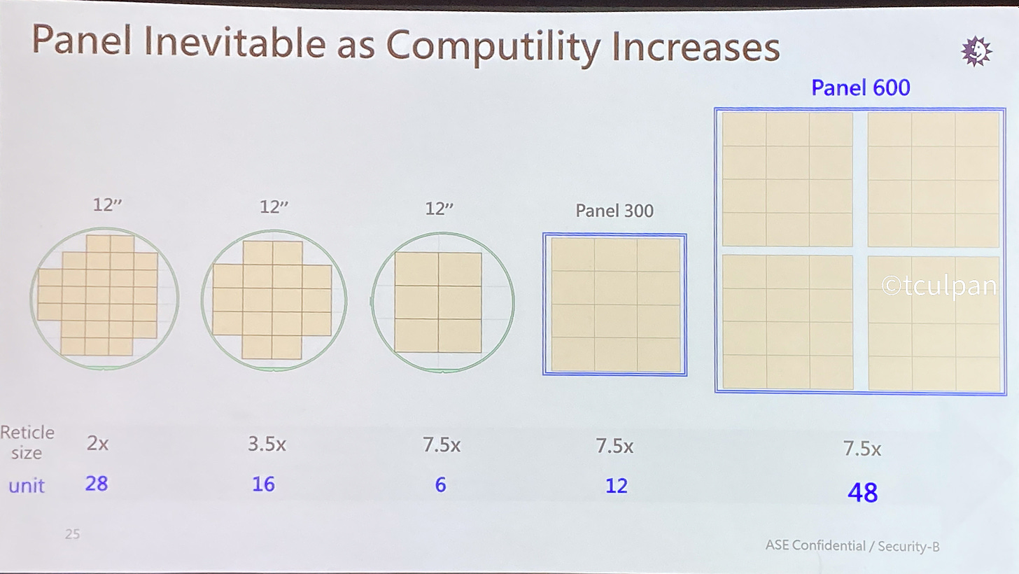
Silicon wafers max out at 12-inches in diameter. High-school maths will tell you that 210mm x 210mm is the largest square you can get from such a shape. That’s not a problem, for now, but it means a lot of wastage when individual chip die sizes get larger, even more so when the entire package (GPU + HBM + other logic) expands. Ever seen a pizza get cut into squares?
Slide shown by Mike Hung, Snr VP, ASE at SEMICON Taiwan, Sept 2024.
This concern has been around for a while. But suddenly chip companies like Nvidia and AMD are demanding larger substrates because there’s a huge performance advantage in having more of their products bonded close to each other in ever-larger packages. HBM, for example, is popular because it’s basically memory glued to the GPU. Old-school computing systems have the CPU and GPU connected to DRAM via wires on a printed-circuit board. But when you’re retrieving, processing and storing billions of bits per second, those few inches are a performance bottleneck. With multidimensional packaging like CoWoS, that gap is measured in microns and nanometers.
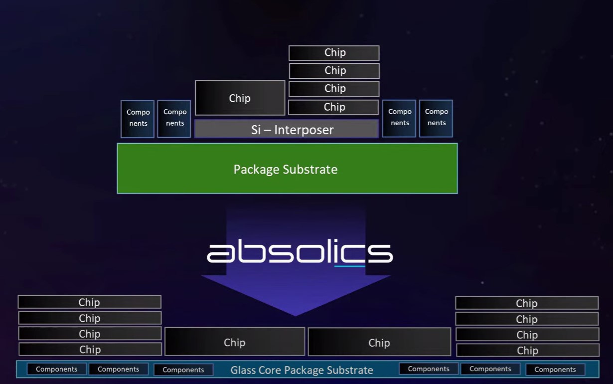
There’s a growing chorus of people who believe that panels of glass are the answer, instead of round wafers of silicon. Size is a key factor. Rather than being limited to a 21cm-square, panels let you go much bigger — 3 meters-square if you like. There’s a few tweaks to the process; some approaches suggest dumping the silicon interposer altogether and instead building the connections onto the glass substrate itself.
This graphic taken from a presentation by Sung Jin Kim, CTO of Absolics, a spin-off from SK Group.
Intel is a big proponent of glass, while Nikkei recently reported that TSMC has started exploring rectangular substrates measuring 510mm x 515mm. (A TSMC executive this week declined to confirm, or deny, to me that the chipmaker has any plans for panel substrates.) Chips themselves will still be made on silicon wafers, but rectangular panels and glass will almost certainly be deployed in the packaging process.
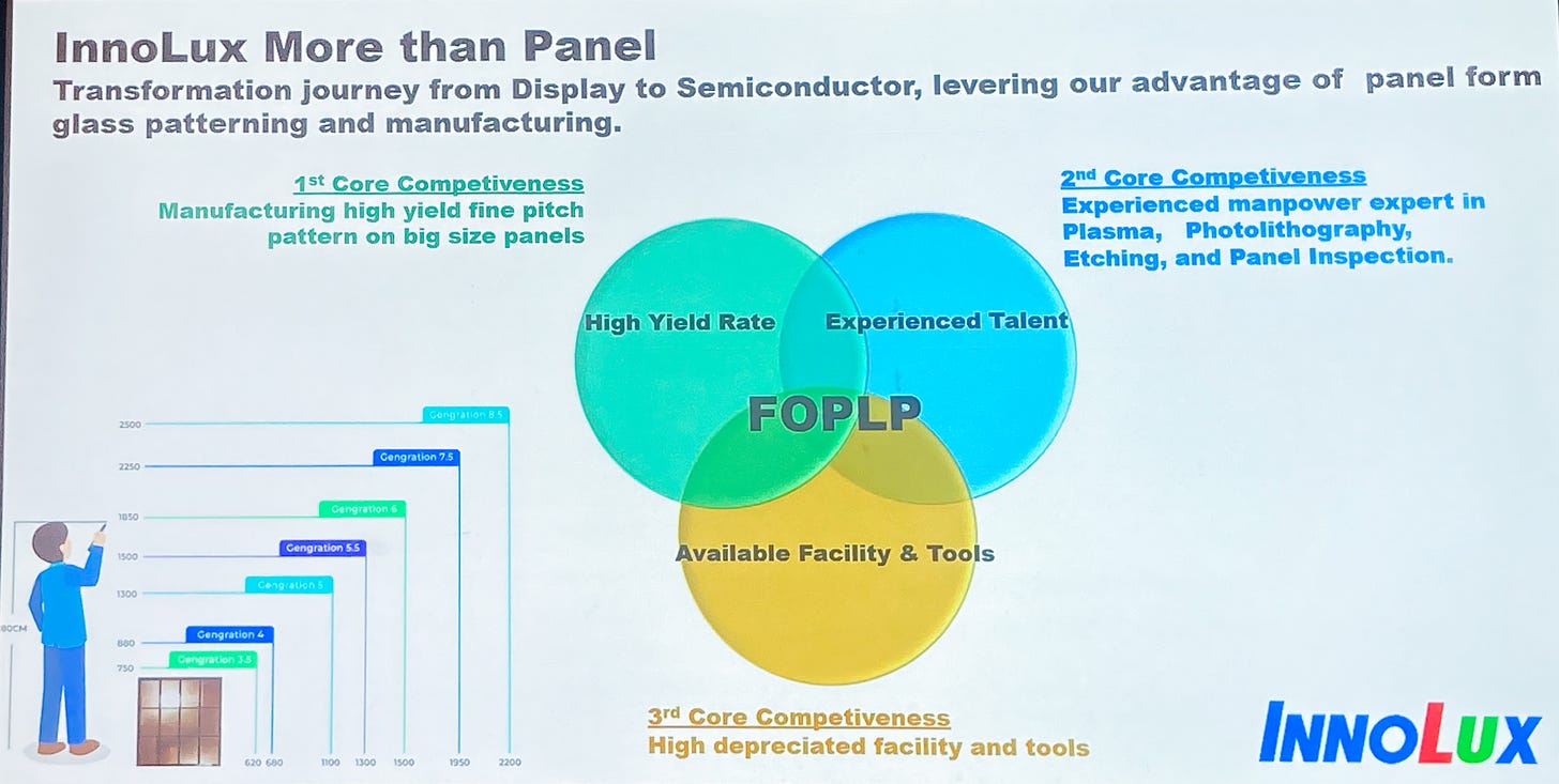
Enter the LCD players, who just so happen to have old factories equipped with tools that can lay microscopic circuitry onto rectangular panes of glass. Even better, they’re staffed with engineers trained to do just that. Many of the challenges semiconductor packagers will face as they transition to panels have already been met and solved by the display-panel industry, including warpage (when substrates bend), mechanical strength, and thermal management.
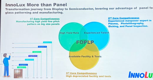
What’s curious about Innolux’s decision to sell its Tainan fab to TSMC is that the company, an affiliate of Foxconn, is itself going big on panel-level-packaging (PLP). It’s already converted three of its 14 LCD fabs to a packaging flavor called fan-out PLP (FOPLP) and is currently in stage two of shifting more capacity away from displays into semiconductors. The Miaoli-based company claims to have the world’s largest FOPLP fab and will earn its first sales from the technology this year. The debut products will include RF chips for satellites and 650 watt EV chargers for US clients.
Slide shown by George Lin, Sr Director of Innolux at SEMICON Taiwan, Sept 2024.
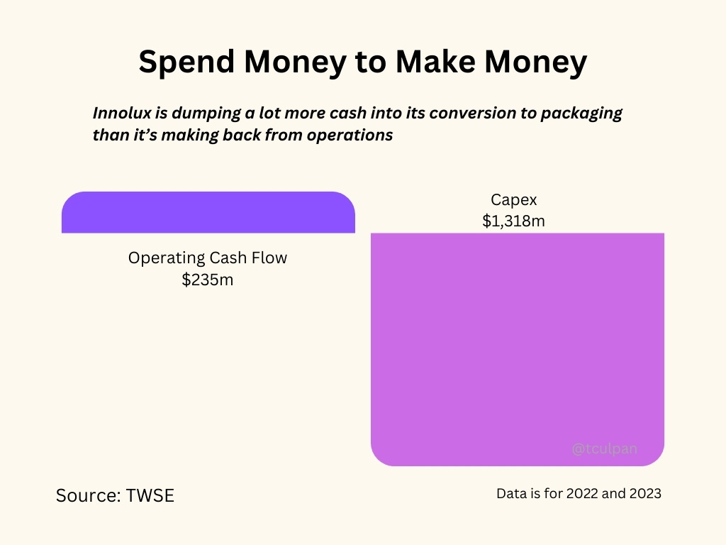
So rather than cut-and-run, Innolux’s factory disposal looks like a case of financial opportunism. It probably doesn’t need all 14 fabs, even if converted to PLP, and there were reports in June that Micron would buy the fab it just sold. So maybe it enjoyed a bidding war, and TSMC paid top dollar. The price of NT$17.1 billion ($531 million) delivered Innolux a bunch of cash and a NT$14.7 billion profit, evidence the facility was almost fully depreciated. Innolux doesn’t seem strapped — it had NT$138 billion ($4.3 billion) in cash at the end of June — but capex outpaced operating cashflow by 5:1 over the past two years, so it makes sense to make hay while the sun shines.
Having watched their contemporaries disappear, AUO and Innolux are being pragmatic enough to sell some of their LCD factories to hungry buyers while they can, and in Innolux’s case find a new use for old factories. The fact that Apple is now dumping LCD in its iPhones altogether proves that this is a wise move.
Chinese giants, like BOE and CSOT, are still in the game and collectively control 70% of the LCD market. Backed by the Chinese government, they may be the last ones able to squeeze any profits from a once-glorious industry before it dies. But at least the technology, and those panel fabs, will live on in the AI era.
Thanks for reading. Rather than pledge a subscription, the best thing you can do is share this piece with three of your smartest friends. And tell them to subscribe. Cheers, Tim.




I am not sure they can without significant government help. But packaging is become a big issue in semiconductors, and Panel-Level is a future trend. I believe there’s a high chance that SMIC or JCET may take a stake in an LCD player like BOE (or vice versa), or some other type of JV/cooperation.
100% BS, LCD is a technology that's always in use, probably will be here until we get something equally practical and easy to manufacture LCD & LEDs of all sizes are and need to be everywhere, might decline? probably, but will always be market for them; but to what other product? there's nothing like it, this is a Lie, so this charlatan can give himself credit